Fueled by fire of innovation, UW collaborators close in on faster chips
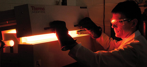
The heat is on in Mike Arnold’s lab.
Furnaces set to 1,800 degrees Fahrenheit blast methane gas over copper substrates to deposit a single layer of carbon-based graphene crystals in a process that may prove more valuable than turning lead to gold.
Yet the heat Arnold and his collaborators feel comes from more than just the furnaces: graphene’s potential to revolutionize the semiconductor industry has ignited the interest of researchers around the world who now are racing to perfect manufacturing processes that capitalize on the hexagonal crystal’s unique properties. At stake is the future of the computer industry, which must find new ways to boost processing speed and memory capacity without consuming proportionately more energy.
Arnold, an assistant professor of materials science, and collaborator Padma Gopalan, an associate professor of materials science, both with the University of Wisconsin-Madison College of Engineering, intend to create a new generation of hybrid computer chips that blend the memory-based capabilities of silicon with the superior logic or fastswitching capabilities of graphene.
To do so, they must overcome a daunting series of technical hurdles that have stymied other scientists whose expertise is concentrated in a single domain. Together, Arnold and Gopalan bring an unprecedented breadth and depth of skill and knowledge that spans polymer chemistry, nanoscale patterning, graphene crystal growth and advanced chip fabrication techniques.
“We’re really pushing the edge of what is currently possible in terms of the manufacturing and performance of a new type of graphene that is semiconducting,” Arnold says. “We believe the possibilities justify the effort. When captured as a single layer of atoms, graphene conducts electricity hundreds of times faster than silicon, the material most commonly found in today’s computer chips, and its flexibility also may allow for exciting new applications in plastic-like electronics, touch screens, or smart tags for merchandise.”
The team’s efforts are being supported by the WARF Accelerator Program, which works to speed the advancement of technologies that hold exceptional promise for commercial success. The program helps inventions clear technical hurdles and advance to the marketplace for the benefit of society.
With the help of several catalysts— seasoned business mentors who contribute insights and ready access to networks of industry leaders—Arnold and Gopalan have developed a four-phase research and development plan that identifies key challenges and benchmarks. Along the way, graduate students Nate Safron from Arnold’s lab and Myungwoong Kim from Gopalan’s lab have contributed to the steady progress. In the first phase of the Accelerator project, the team achieved milestones including fabrication of 1 inch scale graphene samples with perforated holes spaced less than 10 nanometers apart. By comparison, human hair is about 60,000 nanometers in diameter. The perforations are needed to control the interference of electrons across the surface to transform the graphene into a semiconducting material.
While Arnold and his lab team members excel at the methodology to organize the graphene crystals on top of the copper foil, it is Gopalan’s expertise with nanopatterning using polymers that allows the perforations to be formed. Polymers with two components—known as block copolymers—are processed over the surface of the graphene, resulting in the formation of a nanoscale template.
The two components vary in their sensitivity to degradation by ultraviolet light or chemicals. The size of the holes created through the selective degradation can be adjusted at the molecular level based on the combination and length of polymers. To optimize the flow of electrons through the graphene, even the contours of the edges around the holes must be considered in creating the pattern.
“The challenge and excitement in this area comes from our increasing ability to control the size, shape and orientation of the block copolymers through a combination of surface chemistry and thin-film physics,” Gopalan says.
“While mastery of these parameters is crucial to control the flow of electrons and optimize the semiconducting potential of graphene, what we are learning in the process also has other important applications in areas such as catalysis, biofiltration and growth of nanomaterials.”
Once the holes in the polymer have been created, oxygen ions are blasted at the chip. The ions pass through the polymer holes and etch the pattern in the graphene, leaving intact the carbon atoms still covered by the remaining polymer. This remaining grapheme honeycomb can then be transferred to other substrates such as a silicon wafer by dissolving or removing the copper backing and the remaining polymer.
For the graphene to outperform the “ON” and “OFF” switching capabilities of silicon, Arnold and Gopalan must reduce the hole spacing from 10 to 5 nanometers, the width of about 50 atoms. To demonstrate that their work holds commercial potential, they also must prove the process is scalable by expanding the size of the copper substrate holding the patterned graphene beyond the current 2 inch samples to 4 inches. The larger the size, the more difficult it becomes to produce an evenly deposited layer of graphene material.
Given the expected progress, the team is currently seeking an industry partner to explore prototype applications and further scale-up the sample size. Part of the lure for a potential partner comes from the fact that the research already has produced several patent-pending technologies.
Arnold says he and Gopalan recognize that their goal of creating a hybrid graphene and silicon chip represents a significant challenge given the current state-of-the-art. It would be far easier, for example, to identify and pursue an intermediate challenge, such as development of a flexible screen application. Yet, when their research plans were reviewed by the experts on the Accelerator Program Catalyst team, Arnold says the project received resounding support.
“They really encouraged us to go for the gold,” he says. “From a research standpoint, this is fantastic, because if we can achieve that point, it will really transform what computers can accomplish for people. And along the way, there are an awful lot of concepts we will be proving that also hold tremendous potential to benefit society.”