Semiconductors & Integrated Circuits

New Method for Direct Patterning in Block Copolymer Lithography
WARF: P100296US02
Inventors: Padma Gopalan, Eungnak Han
The Wisconsin Alumni Research Foundation (WARF) is seeking commercial partners interested in developing a block copolymer assembly system that combines top-down and bottom-up approaches, includes low molecular weight block copolymer brushes that can be synthesized for most lithography-relevant copolymers and has sufficient sensitivity to enable direct patterning.
Overview
Most microelectronic devices are fabricated using top-down processes such as photolithography. Current top-down processes face growing limitations as the demand for smaller scale applications increases. Alternative approaches are needed to overcome the limitations of existing processes.
Block copolymer (BCP) lithography refers to the use of ordered block copolymer domains in thin-film form as templates for patterning. Self-assembly of block copolymer materials and translation of these ordered domains into thin films has emerged as a powerful approach to create functional nanostructures and templates for various applications.
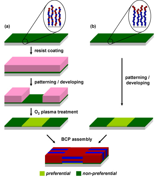
Traditional systems for BCP self-assembly require photoresists, selective etching and an oxygen plasma treatment to create preferential regions between non-preferential regions. The orientation of the domains on the substrate is critical for dictating the pattern geometry for anisotropic domains and control over the orientation requires a non-preferential surface.
Block copolymer (BCP) lithography refers to the use of ordered block copolymer domains in thin-film form as templates for patterning. Self-assembly of block copolymer materials and translation of these ordered domains into thin films has emerged as a powerful approach to create functional nanostructures and templates for various applications.
Traditional systems for BCP self-assembly require photoresists, selective etching and an oxygen plasma treatment to create preferential regions between non-preferential regions. The orientation of the domains on the substrate is critical for dictating the pattern geometry for anisotropic domains and control over the orientation requires a non-preferential surface.
The Invention
UW–Madison researchers have designed a polymer brush that may be used in underlying buffer or imaging layers for block copolymer lithography. These low molecular weight block copolymers (brushes) can be anchored to substrate surfaces to provide a non-preferential buffer layer for the assembly of higher molecular weight block copolymer thin films. The higher lithographic sensitivity of the brushes allows for shorter processing time and a reduction in the number of steps involved with the assembly process. It also allows for more predictable control over the contrast in chemical pattern and provides a lower defect density in the assembled BCP.
This discovery combines bottom-up and top-down approaches into a single system involving depositing a block copolymer solution on a patterned buffer or imaging layer on a substrate and then inducing the BCPs to separate into domains. The direct patterning and assembly approach presents notable simplification with regards to BCP processing.
This discovery combines bottom-up and top-down approaches into a single system involving depositing a block copolymer solution on a patterned buffer or imaging layer on a substrate and then inducing the BCPs to separate into domains. The direct patterning and assembly approach presents notable simplification with regards to BCP processing.
Applications
- Bit-patterned media
- Memory devices
- Nanowire transistors
- Quantum dot arrays
- Photonic crystals
- Photovoltaic cells
- Separation membranes
Key Benefits
- Can be synthesized/tailored for most lithography-relevant copolymers
- Sufficient sensitivity enables direct patterning.
- Requires fewer steps than traditional systems for self-assembly of block copolymers
Stage of Development
The development of this technology was supported by WARF Accelerator. WARF Accelerator selects WARF's most commercially promising technologies and provides expert assistance and funding to enable achievement of commercially significant milestones. WARF believes that these technologies are especially attractive opportunities for licensing.
Additional Information
For More Information About the Inventors
Related Technologies
Tech Fields
For current licensing status, please contact Jeanine Burmania at [javascript protected email address] or 608-960-9846
Figures