Semiconductors & Integrated Circuits

Improved Method for Density Multiplication and Lithography via Directed Block Copolymer Assembly
WARF: P09061US
Inventors: Paul Nealey, Huiman Kang, Francois Detcheverry, Juan DePablo, Ricardo Ruiz, Thomas R. Albrecht
The Wisconsin Alumni Research Foundation (WARF) is seeking commercial partners interested in developing an improved method of lithography utilizing self-assembling block copolymers to increase nanoscale feature density on a substrate surface.
Overview
The creation and replication of nanoscale patterns is becoming increasingly important for the development of new electromechanical, chemical and biological devices at the micro- and nanoscale. For example, the integrated circuit industry relies on optical lithography to etch complex circuit patterns onto silicon wafers. However, the resolution of conventional lithographic techniques is limited by the wavelength of radiation. Even advanced lithographic techniques such as deep ultraviolet or liquid immersion are not able to attain resolution below about 30 nanometers.
Other approaches, such as electron or ion beam lithography, are uneconomical for large scale implementation for several reasons including long etching times and high energy requirements. Therefore, these more expensive techniques are reserved for lithographic mask fabrication, which subsequently can be used to pattern circuits. The ability to easily create patterns smaller than is possible using modern photolithographic methods, on the scale of tens of nanometers and below, will facilitate commercial manufacture of nanodevices and promote their integration into industry as well as the consumer marketplace.
UW–Madison researchers have previously developed an improved method of creating and transferring chemical or physical nanoscale patterns using block copolymers (see WARF reference number P08196US). The method can be used to rapidly and easily generate chemical or physical patterns to be employed in all fields of nanotechnology.
The Invention
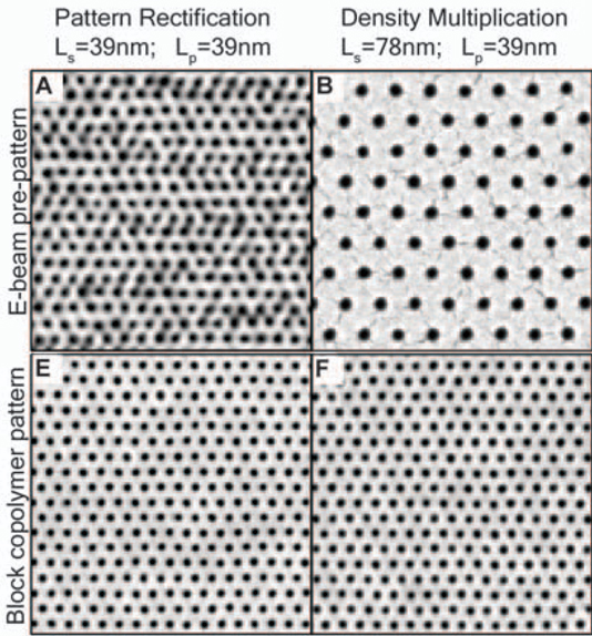
UW–Madison researchers now have developed an improved method to create dense, uniform nanoscale patterns via integration of lithographic techniques and self-assembling block copolymer technology. The method involves chemical patterning, for example by electron-beam lithography, to activate desired regions on a substrate. Then a block copolymer film possessing a specific structure and composition is deposited on the patterned substrate. Upon perturbation of the system, microphase separation of copolymer domains becomes thermodynamically favorable, which generates a second pattern comprising the constituents of the original block copolymer.
The second pattern may have greater density and resolution than the first pattern, depending on the particular block copolymer and desired pattern. In certain applications of the improved method, density can be increased by a factor of four, resolution can be doubled and superior pattern uniformity can be achieved.
When employed with other chemical etching techniques, the improved patterning method can be used to fabricate a substrate possessing one to seven trillion features per square inch with a deviation less than one nanometer from ideal placement. The features patterned on the substrate may include cylinders parallel or perpendicular to the surface, hemispheres or rows. These techniques could be used to manufacture hard drives or similar disk storage systems that could hold much more information per unit area than surfaces prepared by traditional lithographic methods.
Applications
- Manufacture of media disks, magnetic disk drives or similar binary storage devices
- Manufacture of periodic, non-regular or integrated circuit regular fabric architectures by transferring chemical patterns instead of topographic patterns
- Replication of chemical patterns at least an order of magnitude smaller than is possible using existing lithographic technology
- Fabrication of templates or masks for traditional lithography
- Other potential applications include nanoelectronic devices, separation membranes, catalysts, fuel cells and other materials with interesting mechanical, electrical or optical properties
Key Benefits
- Can be integrated into existing nanoscale manufacturing processes
- Improves pattern quality and throughput of current optical lithography techniques
- Reduces cost of manufacture as compared to optical lithography of a similar resolution
- Allows more complicated geometry at the surface than lithographic templates
- Avoids pitfalls of topographic transfer used in nanoimprint lithography
- Can facilitate pattern replication via molecular transfer to secondary substrates
- Can generate a reusable master pattern template to replicate patterns with irregular features
- Increases density by at least a factor of four as compared to optical lithography
- Enhances resolution down to the domain size of block copolymers, approximately five nanometers, which is two to three times greater than optical lithography
- Enhances uniformity with respect to size, placement, vacancies and proximity effects
Additional Information
Related Technologies
Publications
For current licensing status, please contact Emily Bauer at [javascript protected email address] or 608-960-9842
- Ruiz R., Kang H., Detcheverry F.A., Dobisz E., Kercher D.S., Albrecht T.R., de Pablo J.J. and Nealey P.F. 2008. Density Multiplication and Improved Lithography by Directed Block Copolymer Assembly. Science 321, 936-939.
Figures