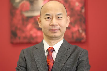
| Meet the University of Wisconsin-Madison’s Jack Ma Professor of Electrical & Computer Engineering |
 |
Research area The advancement of 3-D semiconductor heterostructures from the fundamental level toward practical applications by employing the most diverse types of semiconductors in the world.
What excites you about your work?
“I enjoy doing research, and I’m not short on ideas. Three examples of recent projects include the development of a micro-molded scaffolding photoreceptor “patch” designed to be implanted under a damaged or diseased retina. Once we figured out the recipe, mass production became immediately possible, and commercialization will be very easy. The fabrication methods can be used to create many other types of soft scaffolds for various biomedical applications, such as complicated tissue engineering, etc. A second project, prototyping an ultra-compact laser (called a vertical cavity surface-emitting laser or VCSEL) thinner than 2 micrometers, received WARF Accelerator support. A third project leverages a surprising and inexpensive substance — wood — to make the flexible microwave circuits that power modern communications.”
What do you hope to achieve?
“The patents that I have are broad, and the potential for commercialization is huge. I’m most happy when I can solve a long-lasting problem. Maybe by the time I’m 89 I can realize several more major breakthroughs. I want to leave a mark.”
Jack is advancing research in 3-D semiconductor heterostructures to diversify their applications and increase their capabilities. We believe his work has the ability to change the market.
– Jeanine Burmania, WARF, Senior Director, IP and Licensing
Want to learn more?
Jeanine Burmania, [email protected], 608.960.9846