Engineering
Method for the Growth of Uniform 3-D Nanorod Networks
WARF: P110104US01
Inventors: Xudong Wang, Jian Shi
The Wisconsin Alumni Research Foundation (WARF) is seeking commercial partners interested in developing a method of growing uniform crystalline nanostructures in 3-D spaces, including highly confined spaces.
Overview
Nanotubes and nanowires are used extensively to tailor material properties. However, wide implementation of their extraordinary characteristics has been difficult due to their 1-D geometry and limited length. Fully capturing the promising surface and transport properties of nanostructures in practical devices and systems relies on the ability to translate their 1-D characteristics into 3-D space.
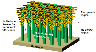
Current techniques for growing single-crystalline nanowires rely on precipitation of precursors. The challenge in these techniques arises from the coupling between crystal growth rate and precursor concentration. Uniform growth of nanowires within confined channels is difficult due to non-uniform distribution of precursors within the channels. Recent advances in 3-D modeling of nanotube networks have clarified the fundamental physics of these structures. However, viable nanofabrication approaches for these architectures have not been realized. A need is felt for a method that overcomes the issues related to coupling between crystal growth rate and precursor concentration during growth of 3-D nanowire networks.
Current techniques for growing single-crystalline nanowires rely on precipitation of precursors. The challenge in these techniques arises from the coupling between crystal growth rate and precursor concentration. Uniform growth of nanowires within confined channels is difficult due to non-uniform distribution of precursors within the channels. Recent advances in 3-D modeling of nanotube networks have clarified the fundamental physics of these structures. However, viable nanofabrication approaches for these architectures have not been realized. A need is felt for a method that overcomes the issues related to coupling between crystal growth rate and precursor concentration during growth of 3-D nanowire networks.
The Invention
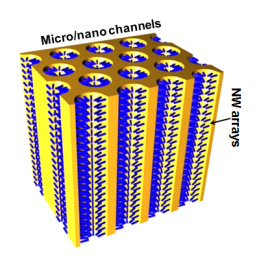
UW–Madison researchers have developed a method for growing 3-D nanorod networks in 3-D spaces, including highly confined spaces. The method is derived from atomic layer deposition (ALD), a state-of-the-art approach that has a growth rate independent of the precursor concentration owing to its self-limiting surface reaction. In this technique, however, higher temperatures and extended pulsing and purging times are implemented to allow networks of nanorods to grow uniformly along the inner surfaces of confined growth spaces.
The method begins by exposing a substrate in a growth chamber to precursor molecules at an elevated temperature, initiating a reaction. Next, the growth chamber is purged of the first precursor and exposed to a second precursor. This initiates a second reaction, after which the growth chamber is purged of the second precursor. These steps are repeated using exposure temperatures and durations such that the reactions result in layer-by-layer atomic construction of crystalline nanostructures within the growth chamber. The resultant interlinking structure may be extensive enough to form a nanostructure capable of maintaining its structural integrity even if the substrate is selectively removed. This is the first and only technique available to grow uniform 1-D nanostructures in 3-D confined spaces.
The method begins by exposing a substrate in a growth chamber to precursor molecules at an elevated temperature, initiating a reaction. Next, the growth chamber is purged of the first precursor and exposed to a second precursor. This initiates a second reaction, after which the growth chamber is purged of the second precursor. These steps are repeated using exposure temperatures and durations such that the reactions result in layer-by-layer atomic construction of crystalline nanostructures within the growth chamber. The resultant interlinking structure may be extensive enough to form a nanostructure capable of maintaining its structural integrity even if the substrate is selectively removed. This is the first and only technique available to grow uniform 1-D nanostructures in 3-D confined spaces.
Applications
- Flow-through photocatalytic membranes
- High performance photovoltaic and photocatalysis electrodes
- Sensors
- Energy storage systems such as lithium ion batteries
- Fuel cells
- Biological mimics of cilia
- Detoxification filters
- Hydrogen storage systems
- Supercapacitors and ultracapacitors
Key Benefits
- Provides a roughness factor of at least 3000, which correlates to increased surface area per unit substrate area
- Allows tunable transport property of electrons, photons and phonons
- Allows improved light absorption
- Enables synthesis of heterogeneous junctions for integration of dissimilar materials, which is essential for solar and photocatalytic applications
- Enables significant performance improvements in many electrical and electrochemical devices
Stage of Development
The development of this technology was supported by WARF Accelerator. WARF Accelerator selects WARF's most commercially promising technologies and provides expert assistance and funding to enable achievement of commercially significant milestones. WARF believes that these technologies are especially attractive opportunities for licensing.
Additional Information
For More Information About the Inventors
Tech Fields
For current licensing status, please contact Michael Carey at [javascript protected email address] or 608-960-9867
Figures